STM32 Black Pill Clone (KiCad)
A from-scratch clone of the popular STM32 “Black Pill” development board, designed end-to-end in KiCad as a hands-on exercise in PCB design: schematic capture through manufacturing file generation. Built following Phil’s Lab’s KiCad tutorial as a structured run through the full workflow.
Overview
The board breaks out an STM32F103C8T6 microcontroller with the peripherals needed to bring it up on a breadboard:
- MCU: STM32F103C8T6 (ARM Cortex-M3, 72 MHz)
- Power: 5 V over USB, regulated to 3.3 V on-board via an AMS1117-3.3 LDO
- Clock: 16 MHz HSE crystal with 10 pF load capacitors
- USB: USB-B Micro for power and communication (with a 1.5 kΩ pull-up on D+ per ST AN4879)
- Programming: 4-pin SWD header (3.3 V, SWDIO, SWDCLK, GND)
- Peripherals: 4-pin UART and I²C headers (1.5 kΩ pull-ups on SDA / SCL)
- Boot select: SPDT slide switch to choose between flashed firmware (RUN) and the internal bootloader (BLDR)
- Mechanical: four M2 mounting holes
Schematic
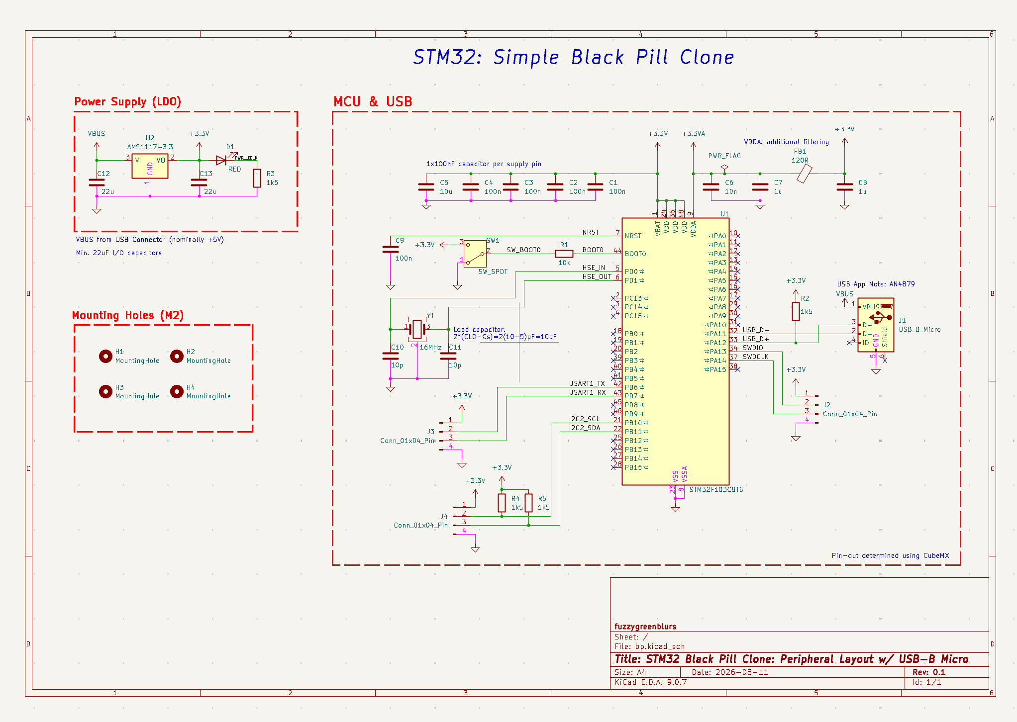
The schematic is organized into three logical blocks:
- Power Supply (LDO). An AMS1117-3.3 linear regulator steps the nominal +5 V USB rail down to +3.3 V, with 22 µF bulk capacitors on both the input and output sides. A red power-on LED with a 1.5 kΩ current-limiting resistor provides a visual indicator that the regulator is running.
- MCU & USB. The STM32F103C8T6 is decoupled with a 100 nF capacitor per VDD pin plus a 10 µF bulk capacitor. VDDA is given additional filtering through a 120 Ω ferrite bead and its own 1 µF and 10 nF caps. Clocking is provided by a 16 MHz crystal with 10 pF load capacitors (sized per
2 · (C_L − C_s) = 2 · (10 − 5) pF). BOOT0 is selected via an SPDT slide switch (with a 10 kΩ pull-down and a 100 nF debounce cap) to choose between running flashed firmware and entering the internal bootloader. USB-B Micro follows the reference design in ST Application Note AN4879, with a 1.5 kΩ pull-up on USB_D+ to identify the device as full-speed to the host. The pin-out was planned in STM32CubeMX, then transcribed onto the schematic. - Mounting Holes. Four M2 mounting holes at the corners for mechanical attachment.
UART, I²C, and SWD are each broken out to a 4-pin header. The I²C lines (PB10 / PB11) carry 1.5 kΩ pull-ups to 3.3 V on SDA and SCL.
PCB Layout
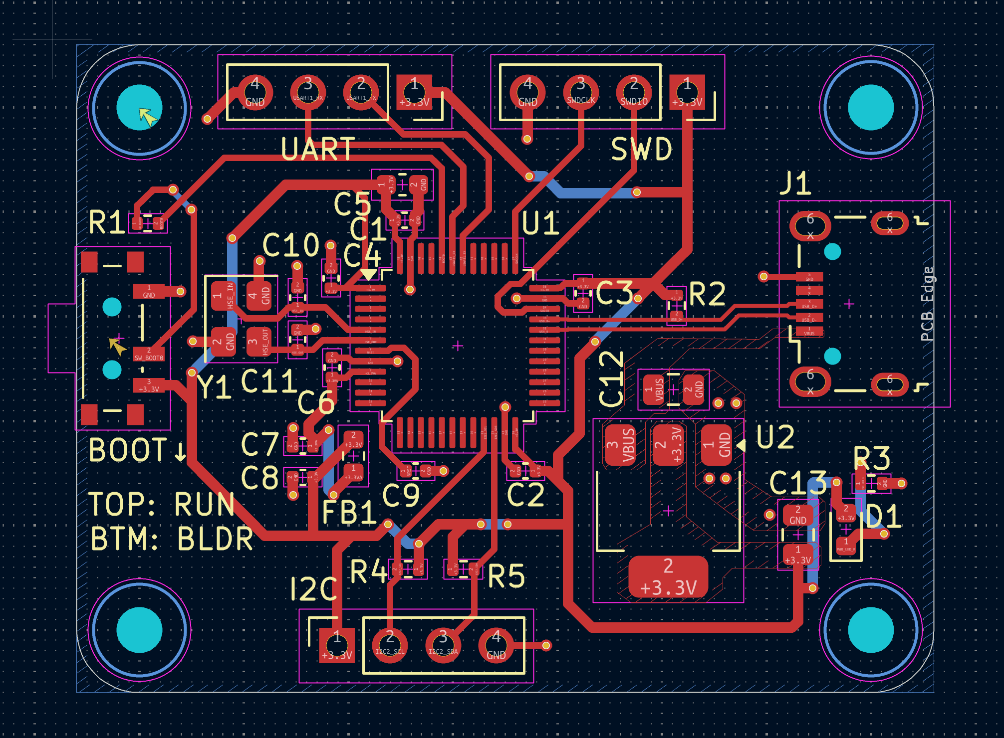
The board is a compact two-layer design. Placement priorities:
- The MCU sits in the centre with its decoupling caps tucked tight against the respective VDD pins to keep loop area small.
- The crystal (Y1) and its load caps (C10/C11) are placed directly next to the HSE_IN / HSE_OUT pins, with a short, tight return path to minimize stray capacitance.
- The USB connector (J1) is on the right edge of the board so the cable enters cleanly, with the USB_D+ pull-up (R2) and a decoupling cap (C3) placed close by. The differential pair is routed as a short matched run from the connector to the MCU.
- The LDO (U2) and its bulk caps (C12/C13) sit in the lower-right, near the USB VBUS entry point, with the power LED (D1) and its current-limiting resistor (R3) at the far corner.
- The BOOT0 slide switch is on the left edge, labeled
TOP: RUN / BTM: BLDRon the silkscreen so the operating mode is unambiguous when handling the board. - The UART, SWD, and I²C headers are arranged along the top and bottom edges so they remain accessible when the board is mounted.
Power and ground are pulled in via wider traces; signal routing uses both layers (red top, blue bottom) with vias to cross over where needed. Four M2 mounting holes anchor the corners.
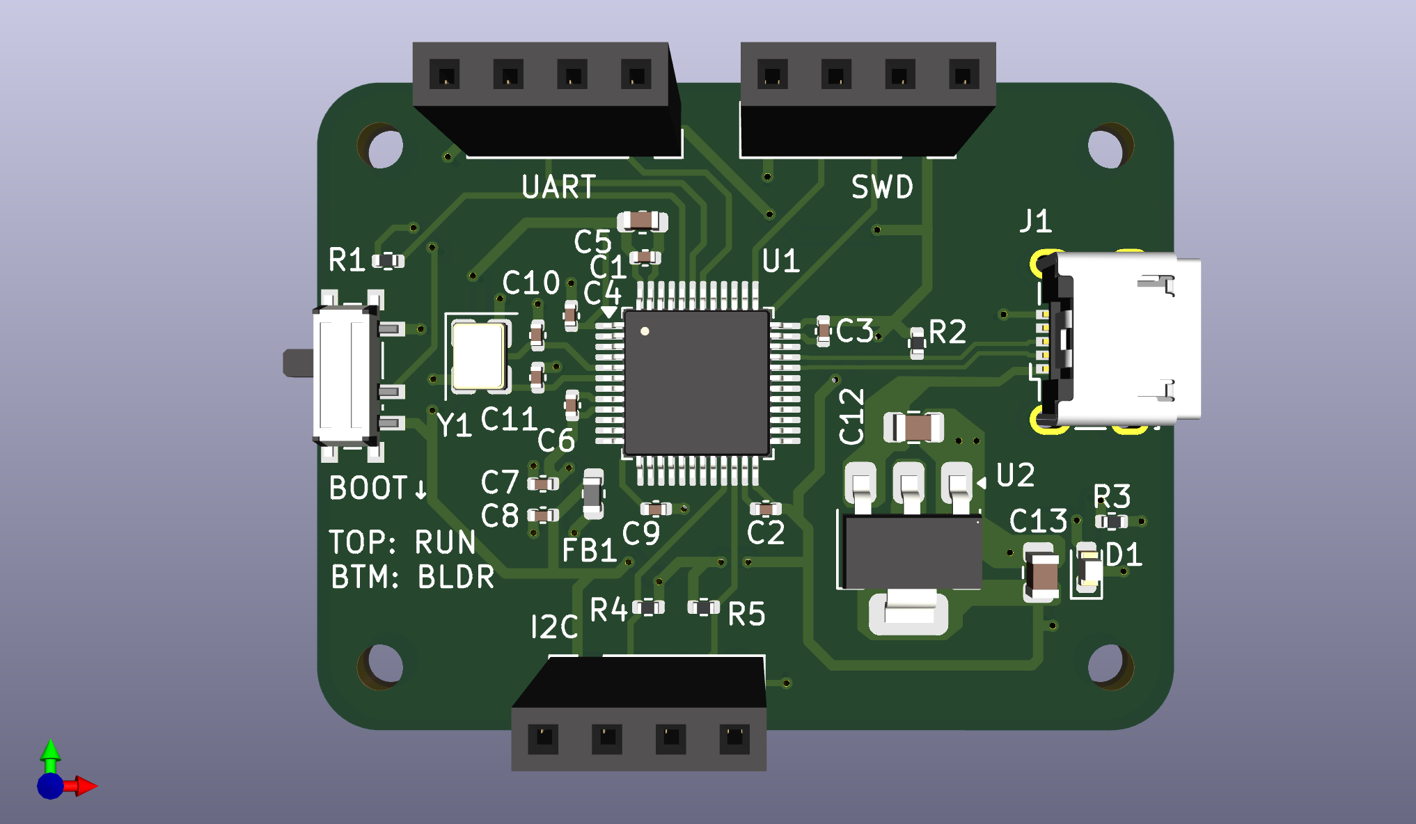
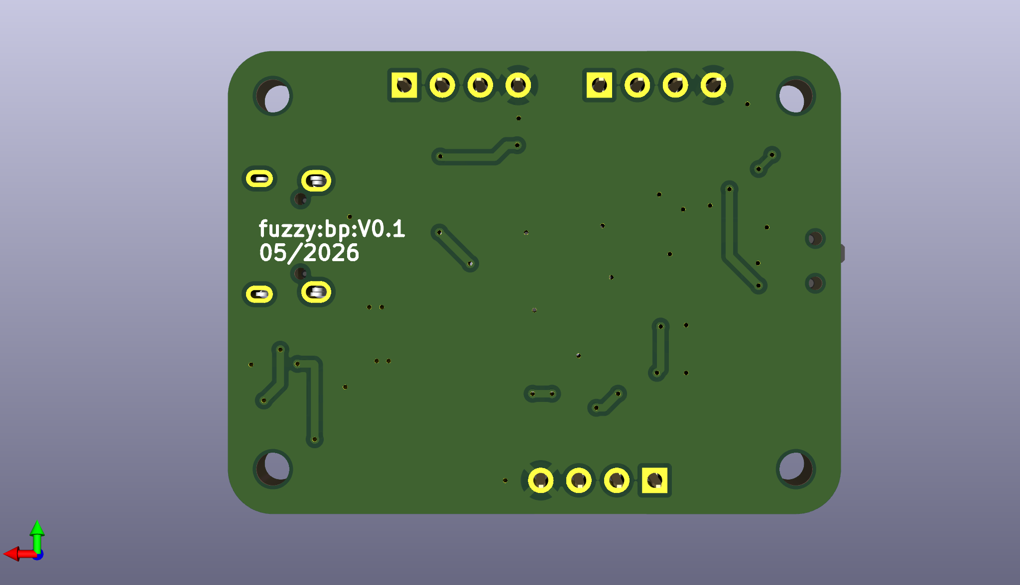
3D CAD Render
A final 3D render of the assembled board using the imported component models, used as a sanity check on connector orientation, silkscreen placement, and overall mechanical fit before sending the design out.
Process
The project followed a full KiCad workflow end-to-end:
- Schematic capture: symbol placement, net naming, ERC, annotation
- Footprint assignment and 3D model verification
- Layout: component placement, footprint adjustments, board outline, mounting holes
- Routing: decoupling and crystal first, then signal nets, then power
- Design Rule Check (DRC) and finishing touches
- Manufacturing output: BOM, CPL, Gerbers, and drill files for fab
Source
KiCad project files, manufacturing outputs, and renders: fuzzygreenblurs/black-pill-clone